TF2 Sentry - Page Work in Progress
Final Schematic and PCB Design
The end goal after designing using the nucleo board was for me to design a PCB board with the STM chip. I've only ever done PCB design for my senior capstone and if you read up on that project, you saw COVID got in the way of the development. I felt this would be a good oppurtunity to learn.
PCB Functionality Design
- Chip
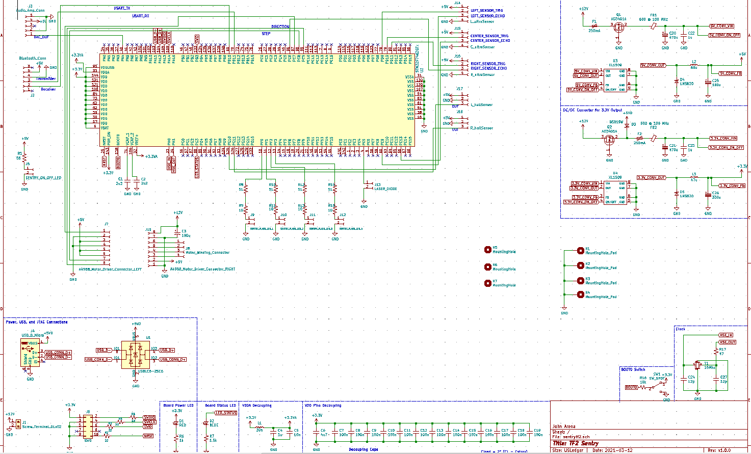
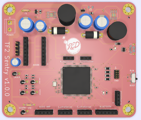
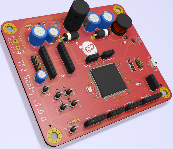
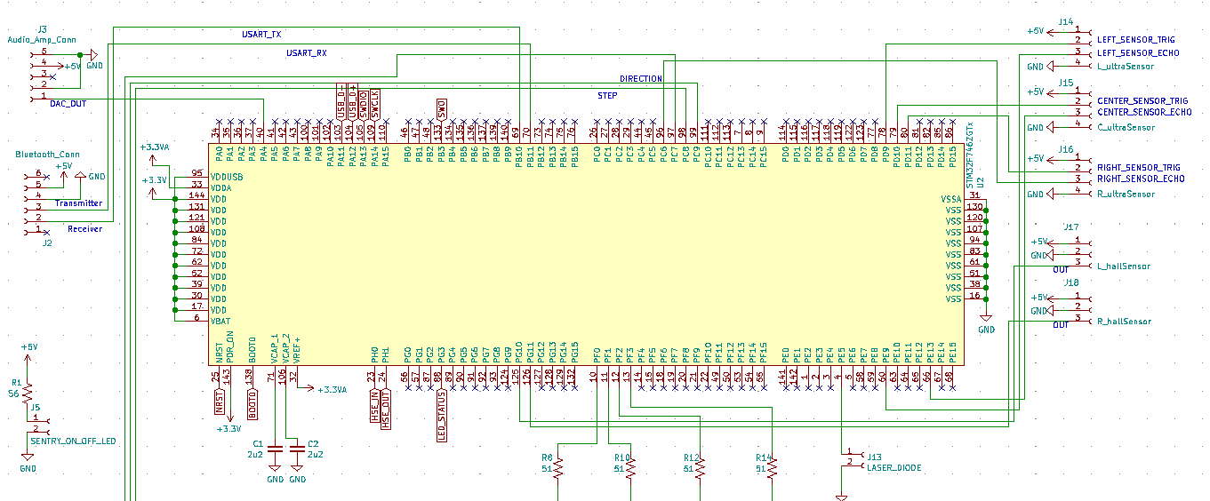
- This is in regards to the STM32F7 chip. I have to find a good spot to place it on the board. My idea I had in mind was to hopefully have it perfectly in the center, but that doesn't end up being the case. It is close to the center though.
- Connectors
- There will be various connectors, male and female, for different reasons. There will be a power connector for the power adapter. There will be adapters for the components such as the ultrasonic sensors. Then there will be USB connectors to connect it to a computer along with JTAG connectors.
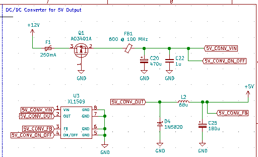
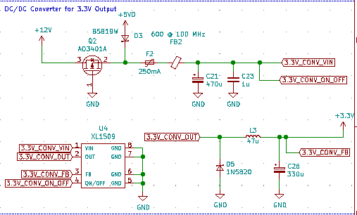
- Power Section
- This will consist of the terminal where I will plug in the 12V power adapter, and two sections that will drop the voltage to 5V and 3.3V. Also, I will have to keep in mind the trace widths for the current ratings. This will be very important on the most current intensive part of the board, the motor controller.
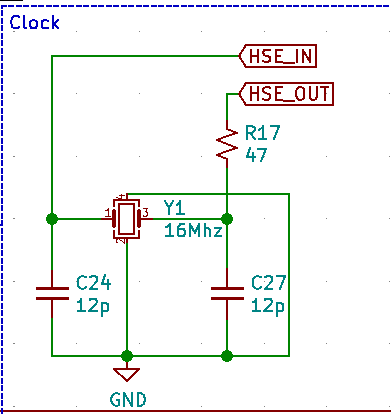
- Clock
- This section will be for the crystal that produces the clock frequency. For my design, I end up using a 16Mhz crystal as the higher frequency crystals will cost an additional fee from JLCPCB, and I'm trying to reduce the costs. This means my code for the STM will have to be updated to reflect using a 16MHz.
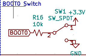
- BOOT0 Switch
- This is for the boot mode. Basically either RUN or PROGRAM mode. Run will run whatever code has been flashed to the board. In SWD, it can override this switch. Since I'm using USB and UART, it wll need a switch. Program will be used to program the board.
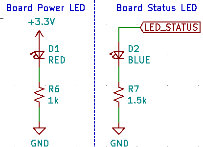
- Board LEDs
- This is straight forward. There will be two LEDs, one for the 3.3V power and one for the board status.
PCB Cosmetic Design
- Shape of PCB
- I wanted to have a circle PCB that will fit the circular shape of the sentry where the PCB will fit. Though I decided to keep it rectangular for now to keep it simple. If I were ever to do a follow up, I'd try to make it a circle.
- RED or BLUE
- Had to decide on which team color. I actually wanted to do a blue color because I have a blue dispenser, but I remember buying the RED colored LEDs and Laser, so I guess it will have to be the RED team.
- Logo
- Obviously since the team color is red, it will have to be the RED logo. I used KiCADs bitmap to component converter to create a component to place on the board. I pulled a picture of the RED logo online and converted it.
The Schematic
- Chip
- This is in regards to the STM32F7 chip. I have to find a good spot to place
it on the board. My idea I had in mind was to hopefully have it perfectly in the center, but that doesn't end up being the case. It is close to the center though.
- Connectors
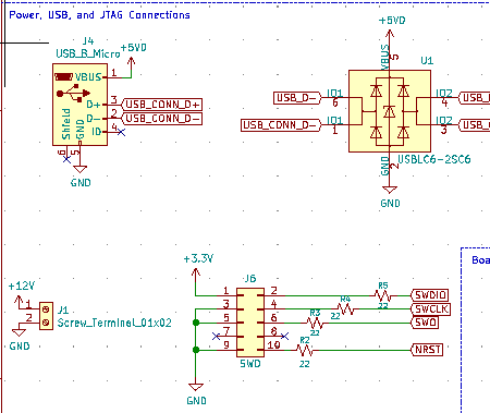
- These are not all the connectors, but here are some. For the power adapter I have a screw terminal. For the SWD I have a 2x5 male adapter. For the USB, I have a USB B micro cable. Along side it is a package that has TVS diodes for ESD protection. It's a good idea since you are unplugging and plugging in the USB a lot onto the board.
- Power Section
- For the power section, I am using XL1509 step down dc/dc converters. It has a wide input range from 4.5-40V and can output up to 2A. Each design is essentially the same with some value changes at the output for the needed values. I have a 5V output for the components like the ultrasonic sensors, bluetooth device, etc. I also have a 3.3V stage for the STM. Both of these take 12V. Now a question occurs of what to do when a 5V input comes from the USB? Well I know when I have the USB plugged in, I'm probably testing and programming. I do not want to be powering anything else other than the board. So first I will only have this for the 3.3V stage for the STM. Obviously I don't want to plug in 12V and then another 5V. Since I have a gate there, I can add an additonal component to create an or gate. I can add a schottky diode that is connected to the 5V from the USB. This creates an essential OR gate for the input stage. Whichever voltage is higher,it will reverse bias the other side. Notice that I specifically use a different 5V power flag for the USB vs the 5V output I'm creating with one of the converters. Otherwise there would be a problem! I also place the fuse after the OR gate since I also have to protect from the USB input. Finally I have some ferrite beads for filtering.
-
- Clock
- I have a 16Mhz crystal that I found on JCLPCB connected accordingly to the data sheet. It's connected to the STM High Speed External input and output pins.
- BOOT0 Switch
- This is for the boot mode. Single Pole Double Throw switch. Meaning it has a single pole and two outputs. Then a 10k resistor for protection and current limiting.
- Board LEDs
- Here I have a LED that comes directly from the 3.3V, meaning the board should be receiving the 3.3V power. The other is a board status LED. I assigned this pin to a GPIO pin and in my code, I can simple say to turn this LED on when the program is running. If the program isn't running for X reason, I will know since the LED isn't on!